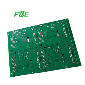
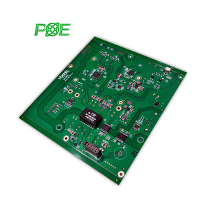
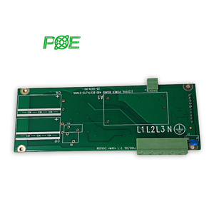
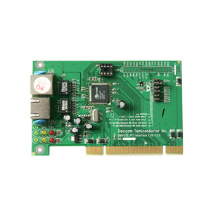
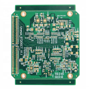
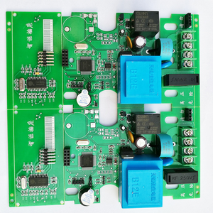
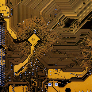
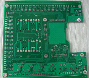
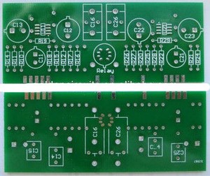
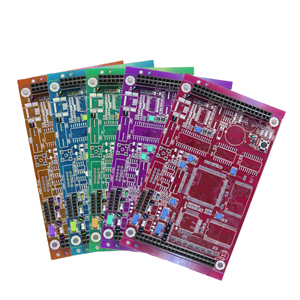
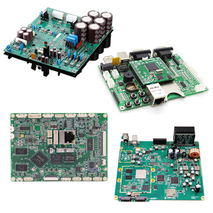
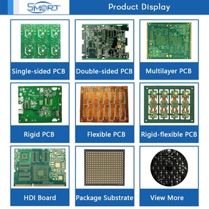
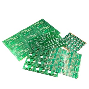
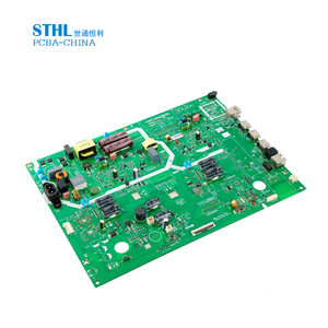
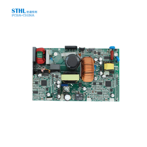
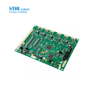
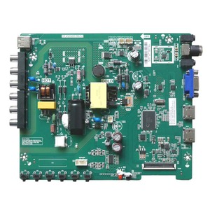
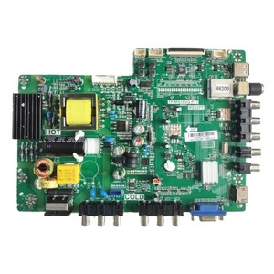
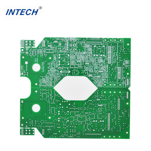
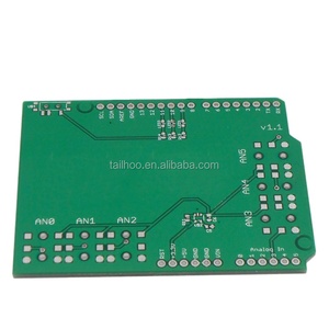
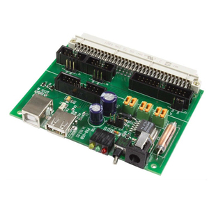
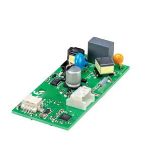
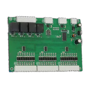
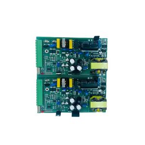
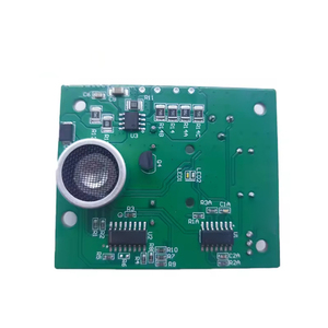
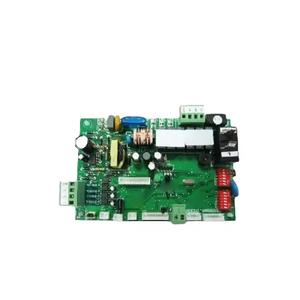
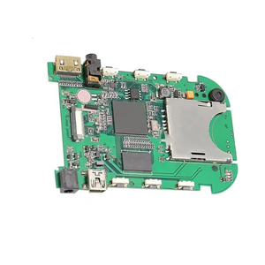
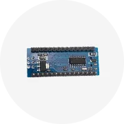
Types of 2-layer PCBs
A 2 layer pcb has various functions due to the diversity of electronic products on the market today. For instance, these circuit boards range from the simple and very low-density interconnect boards to the comparatively more complex medium-density interconnect boards.
High-Temperature PCBs
This type of two-layer PCB is designed to work under very high temperatures. The PCBs are built with materials that can resist heat, so they are predominantly applied in high-end electrical systems like aerospace and automotive.
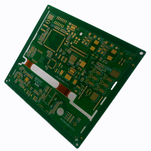
HDI PCBs
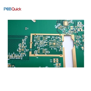
The high-density interconnection (HDI) printed circuit boards are characterized by possessing more lines and a higher component density than a conventional PCB. They feature blind and buried vias and are mainly used in advanced electronics like smartphones and tablets.
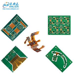
Flexible PCBs
The flexible PCBs are manufactured from some form of glass-reinforced nylon resin (FR-4) to enable flexibility. They are distinctly applicable in space-constrained devices like wearables and medical aids.
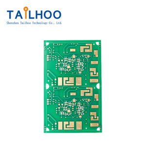
RF PCBs
The radiofrequency PCBs are tailored for high-frequency transmission above 1GHz. They are fabricated from special materials that minimize the loss of signals and are used in wireless communication systems, including cellular networks and satellite systems.
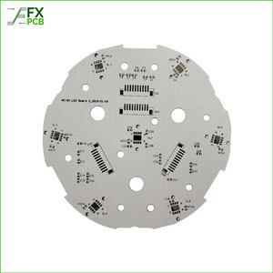
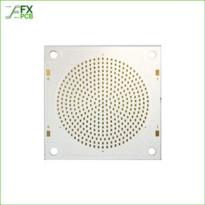
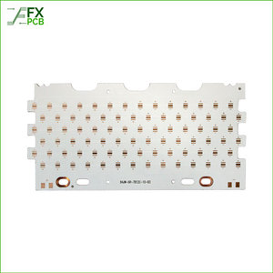
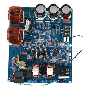
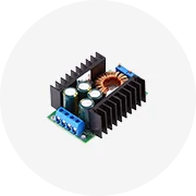
Metal-Based PCBs
The metal-based PCBs come with a metal layer for heat dissipation underneath the two-layer structure. This property makes them ideal for high-power LED systems and other applications generating lots of heat.
Turret PCBs
Turret PCBs are printed circuit boards that have been designed and manufactured with different types of electrical components soldered to protruding terminals or 'turrets', for rugged military, industrial, and other harsh environments.
Copper PCBs
On copper PCBs, a large copper area is used at the base for fast heat conduction away from hot components. Large areas of copper minimize heat build-up on sensitive components and extend device life.
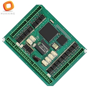
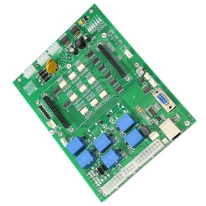
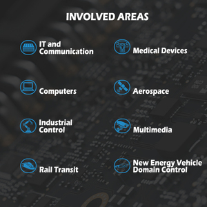
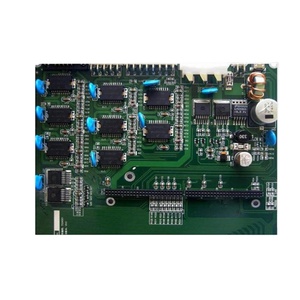
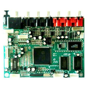
Industrial Applications of 2-layer PCBs
The 2 layer PCBs have many applications in the industrial segment, ranging from control systems to heavy machinery.
Industrial Automation
The 2 layer PCBs are widely used in automation equipment such as programmable logic controllers for industrial settings. Their dual-layer design facilitates the integration of many components necessary for controlling such systems. This feature enhances the automation efficiency in manufacturing processes.
Robust and Durable
As stated earlier, the two-layer printed circuit boards are designed to be very robust and durable. This makes them suitable for the industrial environment, where adverse conditions and frequent mechanical changes are the norm. These characteristic features make them reliable for long periods.
Control Systems
Instrument PCBs are used in control systems, such as monitoring and management systems. The two-layer make of these boards allows for the proper housing of necessary components for signal processing and communication, thereby ensuring effective system control.
Power Distribution
Because the 2 layer PCBs can handle power distribution in industrial gadgets and machinery, they are also suitable for power management systems. Their dual layers allow dedicated power and signal routes, thus facilitating efficient power management in industrial environments.
Sensor Systems
The PCBs are installed on sensor systems; they can house various sensors for monitoring temperature, pressure, and other vital parameters. Their compact and efficient layouts help improve these systems' accuracy and performance.
Heavy Machinery
Two-layer PCBs can be deployed in heavy machinery control systems, including those used in forklift trucks, excavators, and other heavy mobile equipment. They can withstand vibrations, pressure, and temperature changes, making them suitable for such a demanding environment.
Cost-Effective Solution
In industries where the scale of production is high, the usage of 2 layer PCBs ensures a reduced cost, which is beneficial. These can lead to overall cost savings for companies without sacrificing quality.
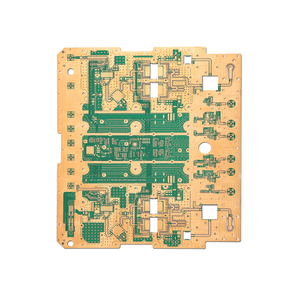
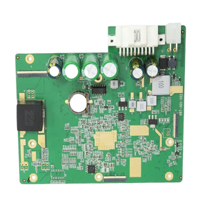
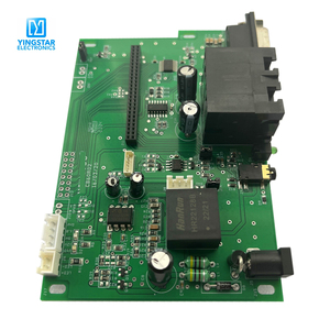
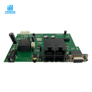
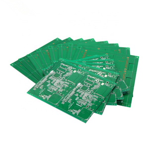
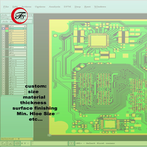
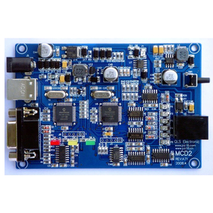
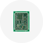
Product Specifications and Features of a 2-layer PCB
Like all printed circuit boards, the 2 layer PCB has unique features and specifications that allow it to perform its functions. There are also many considerations regarding the material used to manufacture it and its thicknesses and applications.Material Specification
-
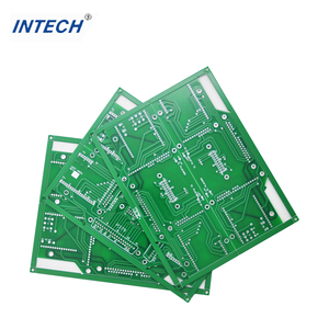
FR-4
The vast majority of 2 layer PCBs are constructed of FR-4, a glass-reinforced epoxy resin. Due to its great mechanical strength and chemical resistance, it has become a popular choice.
-
Coppert
Copper is the most popular metal used to construct 2-layer circuit boards due to its high conductivity for making tracks and pads. PCBs come in varying copper thicknesses ranging from half an ounce to several ounces per square foot, depending on the electrical needs of the application.
-
Additional Materials
Other materials used can be polyimide for high-temperature applications and aluminum or copper for PCBs requiring efficient heat conduction.
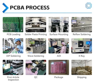
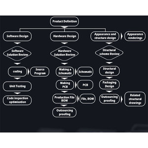
How to Install
-
Design Preparation
The production of a 2-layer PCB begins with the design stage. It deals mainly with the two-layer layout that will be printed on the circuit board. Hence, it is prepared using a PCB design software.
-
Layer Alignment
In the PCB manufacturing process, the two layers of the board are aligned tight and together. This is necessary for both layers to be designed fabricated for proper electrical connectivity.
-
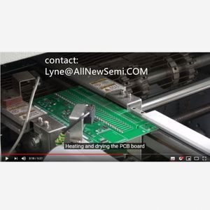
Etching
The manufacturers of the PCB use a process known as etching to remove excess copper from the layered material and reveal the circuit pattern. The etching process itself requires a chemical or a laser, depending on which method was chosen.
-
Drilling Vias
After etching the layers, vias or small connections between the two layers, will need to be drilled. This is done to enable interconnectivity to enhance electrical flow between different sections of the PCB.
-
Solder Mask Application
A solder mask is applied on the PCB to protect the copper traces. This also helps to prevent solder bridges during the component soldering process, which could knock out the board.
-
Component Installation
This last step, installation, involves soldering all the electronic components onto the provided pads on the PCB to complete the circuit board.
Maintenance and Repair
-
Maintenance
For proper maintenance of 2-layer PCBs, frequent inspection and cleaning, temperature monitoring, and preventive component replacement must be performed. These helps in preventing board failure and extending its operational lifetime.
-
Repir
The general repairs on the PCBs include replacing its damaged components, re-soldering bad joints, and in cases of very massive destruction, incorporating repairs with the aid of flexible or conductive adhesives.
Product Upscale
The 2-layer printed circuit boards can be upscaled by increasing its copper thickness, using high-quality materials for enhanced flexibility, heat resistance, or electrical performance, increasing the layer counts to high density interconnects.
PCB thickness and layer specifications
The standard thickness for a 2-layer PCB is 1.6mm, although it can vary from 0.2 to 3mm depending on application requirements. They support copper thickness ranging from 0.5 to 5 mils, which is 1 to 125 microns, per layer.
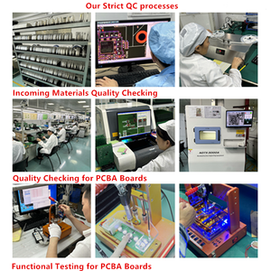
Quality and Safety Considerations of 2-layer PCsbs
The quality and safety of any product that employs a 2-layer PCB directly affect the PCB's reliability, durability, and performance. Thus, quality considerations include material selection, manufacturing precision, and adherence to international standards.
Quality Considerations
-
Material Selection
The 2-layer PCBs should be constructed using top-quality materials such as copper and FR-4. PCBs made of substandard materials will ultimately lead to poor conductivity and board failure.
-
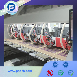
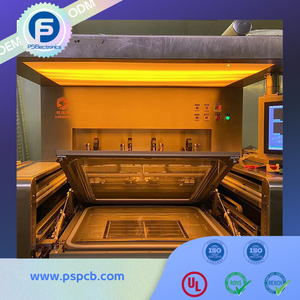
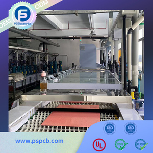
Manufacturing Process
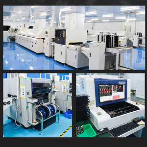
The process entailing high precision and modern equipment in 2-layer PCB manufacturing should be emphasized. Only then can the chances of defects be reduced, which further increases the board's reliability. Quality assurance is thus performed through systematic inspections during all manufacturing stages.
-
Component Placement and Soldering
The proper placement and soldering of components are needed to maintain quality. This is to ensure good electrical connectivity and no incidences of failing components due to poor soldering or placement.
-
Testing
Many manufacturers perform electrical testing, such as continuity checks and functional tests, to ascertain that the 2-layer PCBs meet acceptable standards. This is a commonly used high-quality maintenance technique.
Safety Considerations
-
Fire Hazard Deminishing
PCBs often come applied in gadgets that can be prone to overheating. Such PCBs must be manufactured with materials that can withstand heat and, at the same time, reduce the chances of fire. They also include proper heat dissipation, especially for PCBs used in heavy electrical and mechanical devices.
-
Proper Handling Measures
Manufacturers must properly handle PCBs to avoid electrostatic discharge (ESD), which can destroy sensitive components. Adopting proper ESD controls will reduce product failure and improve safety.
-
RoHS Compliance
For safety, it will be best to use PCBs made by components that conform to the directive on hazardous substances (RoHS). This requires that processes or materials containing lead, cadmium, or other hazardous chemicals be eliminated.
-
Quality-Driven Testing
The reason for performing quality-driven testing is to address safety concerns. Typical tests include checking for short circuits, heat resistance, and the emission of harmful substances.
Q&A
Q1. What makes people prefer 2-layer PCBs?
A1. 2-layer PCBs are preferred because of their relatively low production costs, versatility, uncomplicated complexity, and effectiveness for a multitude of general electronics.
Q2. What is the maximum frequency that can be used on a 2-layer PCB?
A2. A 2-layer PCB can be used for various applications and is typically used at frequencies up to 1GHz. However, if manufactured from superior materials, it can handle up to 3GHz.
Q3. What is the difference between a 2-layer PCB and a 4-layer PCB?
A3. A 2-layer PCB has two layers of conductive material, while a 4-layer PCB has four layers. The 4-layer PCB is used for more complex circuits with higher component density and multilayered connections.
Q4. Are 2 layered PCBs flexible?
A4. The 2-layer PCBs are not flexible. Only if one of the layers is made of a flexible substrate like polyimide will the 2-layer PCB possess flexibility.
Q5. What are some of the negatives of a 2-layer PCB?
A5. The 2-layer PCB disadvantages include limited application in high-density circuits, restricted multilayer interconnections, and comparatively more power usage than high-density interconnection.


 浙公网安备 33010002000092号
 浙B2-20120091-4